Towards fibre-like loss for photonic integration from violet to near-infrared
Summary
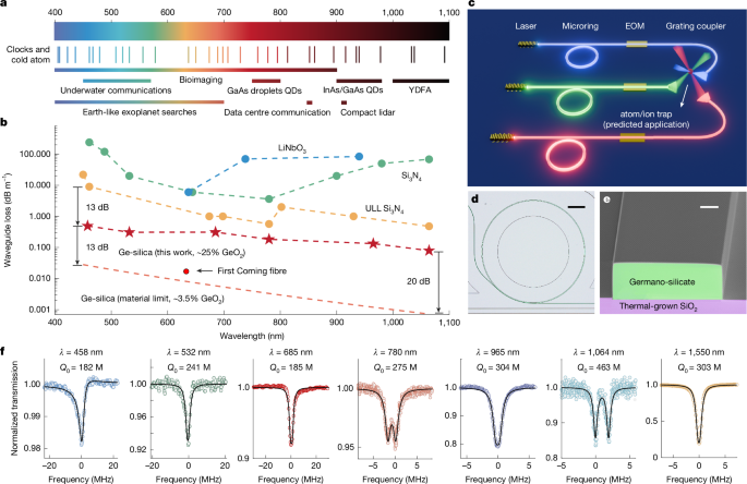
This Nature paper presents a germano-silicate (Ge-silica) planar photonic platform that achieves fibre-like, ultralow waveguide loss across the visible to near-infrared (458–1,550 nm). Using a DUV-stepper lithography flow and PECVD-deposited GeO2-doped silica, the team fabricate high‑Q microring resonators with intrinsic Q factors exceeding 180 million across a broad spectrum and a peak Q of 463 million at 1,064 nm (equivalent to ~0.08 dB m−1 loss).
The process leverages Ge-silica’s low material absorption and its low-viscosity reflow at standard furnace temperatures to produce atomic-scale smooth sidewalls and suppress Rayleigh scattering at short wavelengths. The platform demonstrates both annealed and anneal-free devices (the latter still giving ultrahigh Q), is CMOS-compatible and supports thick (>4 µm) waveguides for large mode areas that reduce thermorefractive noise. Key demonstrations include single-ring soliton microcombs, stimulated Brillouin lasing (enabled by simultaneous optical and acoustic confinement) and self-injection-locked narrow-linewidth lasers with Hz-level fundamental linewidths across visible and NIR wavelengths.
The authors discuss practical advantages and trade-offs (lower index contrast → larger bending loss) and outline routes to further reduce loss toward the material limit, potentially enabling PICs with fibre-like losses for clocks, quantum systems, microcombs, gyroscopes and other high-performance photonic systems.
Key Points
- Ge-silica waveguides fabricated by DUV-stepper lithography achieve sub-dB m−1 losses from violet to telecom bands; record low loss: 0.49 dB m−1 at 458 nm and 0.08 dB m−1 at 1,064 nm.
- Microring resonators show intrinsic Q >180 million across 458–1,550 nm, peak Q ≈463 million at 1,064 nm.
- Surface-tension-induced reflow smooths sidewalls to atomic scale, overcoming short-wavelength Rayleigh scattering limits in PICs.
- Platform is CMOS-compatible, supports anneal-free ultralow-loss devices (important for temperature-sensitive heterogeneous integration).
- Material advantages: GeO2 doping raises refractive index for confinement, lowers acoustic velocity enabling simultaneous optical and acoustic mode confinement—demonstrated by Brillouin lasing.
- Large-mode-area (thick) waveguides reduce thermorefractive noise, enabling Hz-level self-injection-locked lasers across visible and NIR wavelengths.
- Demonstrations include single‑ring anomalous-dispersion soliton microcombs, high-coherence Brillouin lasers and low-noise hybrid-integrated diode lasers; potential to reach material-limited loss with further process improvements.
Author’s take
Punchy: This is a platform-level advance. The paper doesn’t just nibble at visible‑band loss limits — it demonstrates a realistic path to bringing fibre-like loss onto a planar, CMOS-compatible chip. If you’re involved in integrated lasers, quantum photonics, microcombs or on‑chip sensors, the full methods and demos are worth the read because they change what’s practicable on chip.
Why should I read this?
Short version: they’ve shown you can get near‑fibre loss on a chip from violet through the NIR — and they back it up with real devices (microcombs, Brillouin lasers, Hz‑level SIL lasers). If you care about low noise, narrow linewidths or bringing fibre-grade performance into PICs without exotic suspension tricks, this paper saves you months of digging and gives concrete process steps and demonstrations.
Context and relevance
This work addresses a major bottleneck in visible and short‑NIR integrated photonics: rising scattering and absorption as wavelengths shorten. By using germano‑silicate, DUV fabrication and thermal reflow, the platform sidesteps those limits and enables multi‑material integration (III–V, LiNbO3, detectors) with low thermal budget and long‑term stability. The result is directly relevant to atomic/ion control chips, integrated optical clocks, quantum networks, low‑noise microwave photonics, on‑chip lidar and precision sensors — essentially moving many fibre‑based technologies onto foundry‑compatible PICs.