Microsoft’s Maia 200 promises Blackwell levels of performance for two-thirds the power
Author note
Author style: Punchy — this is a big play in AI infrastructure and worth paying attention to if you care about inference costs and scale.
Summary
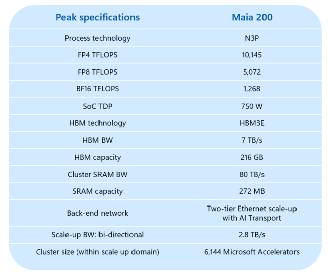
Microsoft has unveiled the Maia 200, a purpose-built inference accelerator fabricated on TSMC’s N3 node. The chip packs 144 billion transistors and delivers about 10 petaFLOPS of FP4 compute while drawing 750W. Microsoft claims Maia 200 is optimised for inference of very large models, offers higher efficiency and lower cost than existing AI silicon, and can scale across thousands of chips using an integrated Ethernet network-on-chip and Microsoft’s AI transport layer.
Key Points
- Maia 200 is an inference-optimised accelerator built on TSMC N3 with 144 billion transistors and ~10 petaFLOPS (FP4) peak.
- It has 216GB of HBM3e (likely six stacks) delivering a claimed 7TB/s memory bandwidth.
- Power draw is 750W, significantly lower than many competing Blackwell GPUs (which can exceed 1,200W), and Microsoft says Maia is ~30% cheaper than other AI silicon today.
- Hardware tensor units support low precisions (FP8, FP6, FP4) — excellent for inference but incurs penalties for higher-precision training workloads.
- Scale-up design: chips can cluster to 6,144 units delivering ~61 exaFLOPS and 1.3PB HBM3e, using an on-chip Ethernet NoC and a two-tier scale-up topology.
- On-chip SRAM (272MB) can be partitioned into CSRAM and TSRAM to reduce HBM traffic and improve collective communications.
- Maia 200 is already running in Microsoft’s Central (Des Moines) region; an SDK preview supports PyTorch and Triton kernels for early adopters.
- Despite Maia’s strengths, it is an inference-focused part — Microsoft will likely continue to use Nvidia GPUs for training and other mixed workloads.
Content summary
Maia 200 is positioned as Microsoft’s second-generation in-house AI chip, aimed squarely at inference for very large language models. With a focus on low-precision tensor compute and high memory bandwidth, the design choices favour interactive token throughput and efficiency per watt. By limiting hardware tensor support to FP4/FP6/FP8, Microsoft squeezes performance and power savings but sacrifices versatility for high-precision training tasks. The chip’s network-on-chip and transport layer enable very large cluster scale-up, making it suitable for hosting frontier models in Azure. Microsoft is marketing Maia as cheaper and more power-efficient than existing options, while acknowledging the chip’s specific focus on inference rather than general-purpose GPU workloads.
Context and relevance
This announcement matters because it signals intensified competition in AI infrastructure beyond Nvidia’s GPU dominance. Cloud providers building custom accelerators can reduce operating costs, improve density and lower energy consumption for inference-heavy services. For organisations running large-scale inference (chat, search, retrieval-augmented generation), Maia 200 could materially cut cost-per-token and datacentre power bills. However, its inference-only orientation means training fleets and mixed workloads will still favour GPUs that support higher precision and broader software ecosystems.
Why should I read this?
Short answer: if you pay cloud bills for LLM inference or run large-scale AI services, this could change the economics. Maia 200 might slash power and hardware cost for inference-heavy workloads — so it’s worth knowing what trade-offs Microsoft has made to get those savings and how that affects model performance and deployment choices.
Source
Source: https://go.theregister.com/feed/www.theregister.com/2026/01/26/microsoft_maia_200/