
Large-scale analogue quantum simulation using atom dot arrays
Article Date: 2025-01-16
Article URL: https://www.nature.com/articles/s41586-025-10053-7
Article Image: Figure 1 (STM image)
Summary
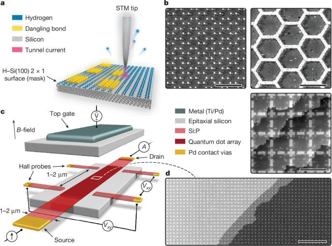
This paper demonstrates large-scale analogue quantum simulation using atom-based quantum dots fabricated by STM hydrogen lithography in silicon. The team patterns 100 × 150 square-lattice arrays containing about 15,000 dopant-defined quantum dots, integrates them into an epitaxial Hall-bar device with metallic leads and a top gate, and performs low-temperature magneto-transport and bias-spectroscopy measurements.
The authors engineer and tune Hubbard-model parameters — on-site interaction U, inter-site interaction V, tunnelling t and electrochemical potential μ — by varying dot spacing (7.2–17.1 nm) and dot area (9–62 nm2). By quenching t and changing U/t across devices A–F they observe a metal–insulator (Mott–Anderson) transition, measure interaction-enhanced charge gaps, identify a two-step thermal activation consistent with incoherent→coherent cotunnelling, and report temperature-dependent Hall-coefficient behaviour suggestive of Fermi-surface reconstruction in the weakly insulating regime.
The work highlights sub‑nanometre precision STM patterning at micrometre scales (via advanced STM controller corrections), substantial next-nearest‑neighbour Coulomb interactions, and the ability to implement arbitrary 2D lattice geometries (hexagonal, Lieb, honeycomb) for future studies of correlated phases including potential superconductivity and topological states.
Key Points
- Fabricated 100 × 150 arrays of atom-based quantum dots (≈15,000 dots) using STM hydrogen lithography with micron-scale precision corrections.
- Integrated arrays into an epitaxial Hall-bar device with metallic (Ti/Pd) top gate and ohmic leads to enable transport and Hall measurements.
- Tuned inter-dot spacing (7.2–17.1 nm) and dot area (9–62 nm2) to vary U, V and t; achieved U/t values from ≈14 up to ≈203.
- Observed a clear metal–insulator (Mott–Anderson) transition across device series; identified a critical conductance σc ≈ 1.11 (2e2/h).
- Bias spectroscopy shows Coulomb and Mott–Hubbard gaps and interaction-strength-dependent coherence peaks across devices.
- Magnetic-field data reveal exchange-enhanced charge-addition energies and an interaction-related effective g-factor, enabling extraction of a dot spin susceptibility χs that scales with U and dot size.
- Low-bias conductance shows two-step thermal activation (inelastic → elastic cotunnelling) following an Efros–Shklovskii law with device-dependent activation temperatures.
- Temperature-dependent Hall coefficient in conductive devices reveals carrier freeze-out trends and, in the weakly insulating sample, low-temperature anomalies consistent with Fermi-surface reconstruction or miniband formation.
Why should I read this?
Short version: these folks just built the biggest, cleanest dopant-defined quantum-dot simulator yet and used it to watch a Mott–Anderson switch flip. If you care about real-world platforms that can emulate strongly correlated electron physics (think superconductivity, strange metals, topological matter) without resorting to ultracold atoms or moiré stacks, this is the one-page shortcut — clever fabrication + direct transport probes = a proper roadmap for large-scale analogue simulation in silicon.
Author note
Punchy take: this is a significant step. Achieving 15,000 atom-defined dots with controlled U/t and performing comprehensive magneto-transport demonstrates a scalable, versatile platform. The results are directly relevant to experimentalists and theorists working on Hubbard-like models, mesoscopic Coulomb effects and engineered quantum materials; the ability to pattern arbitrary 2D lattices opens experimental routes that are hard or impossible in other platforms.