The Ridiculously Nerdy Intel Bet That Could Rake in Billions
Summary
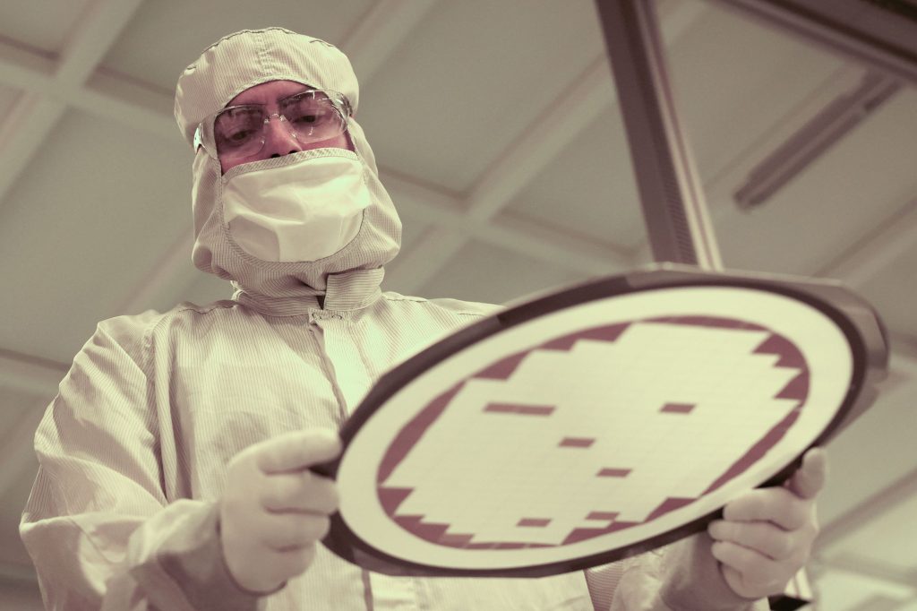
Intel is betting heavily on advanced chip packaging as a major growth engine in the AI era. The company has reactivated and invested in fabs such as Fab 9 in Rio Rancho, New Mexico, and is rolling out new packaging technologies (EMIB, Foveros and the newer EMIB-T) that stitch multiple chiplets together to improve performance, power efficiency and signal integrity. Intel’s Foundry arm is pitching packaging as a service to outside customers — including reported talks with Google and Amazon — and executives expect packaging revenue to climb into the billions, potentially before wafer revenue scales up.
The strategy positions Intel against TSMC, which dominates wafer production and already offers integrated packaging services. Intel argues its approach is more “surgical”, offering customers flexibility to “enter and exit the highway” at different stages of the manufacturing process. Success hinges on winning third-party deals, expanding packaging capacity (including plans in Malaysia), and sustained capital expenditure to scale operations — all while managing environmental and local concerns around fab expansions.
Key Points
- Advanced packaging combines multiple chiplets into a single package to increase density, bandwidth and efficiency — critical for AI workloads.
- Intel developed EMIB and Foveros technologies and is deploying EMIB-T to improve power and signal performance between components.
- Intel’s Foundry is positioning packaging as a revenue stream that could reach well north of $1 billion and potentially achieve high margins.
- The company is courting large cloud/custom chip customers (reports name Google and Amazon) to provide packaging services even if those customers source wafers elsewhere.
- Scaling packaging is hard: it requires fab capacity, specialised processes and significant capital investment — plus customers may wait to see proof before announcing partnerships.
- Intel is expanding capacity in New Mexico and Malaysia; local environmental and resource concerns (eg. water use, emissions) are part of the debate.
- Packaging could reshape competitive dynamics: if Intel wins customers, it can monetise backend services even while TSMC leads on wafer fabrication.
Context and Relevance
Why this matters: AI is driving demand for specialised chips that need more memory, bandwidth and bespoke interconnects — things packaging directly addresses. As hyperscalers design custom silicon but rely on foundries for parts of the process, packaging becomes a valuable outsourced service. Intel’s push reflects a broader industry trend: the wafer front end and the packaging back end are both strategic battlegrounds. For investors, suppliers and cloud providers, packaging deals and capacity expansions are leading indicators of who will control the next phase of AI infrastructure.
Why should I read this?
Because it’s the boring, nerdy bit that actually decides who makes the cash when AI goes big. If you want to know where the real margins and strategic leverage are hiding — not just in flashy GPUs but in the way chips get put together — this story saves you the slog. Intel’s packaging play could shift supply chains, profits and power in AI hardware. You’ll want to know whether they can pull it off.
Author style
Punchy. This piece spotlights a technical, high-stakes wager that could be massively consequential — so treat the detail as meaningful intel. If Intel nails packaging and signs major cloud customers, the ripple effects will matter to hardware makers, cloud operators and investors alike.
Source
Source: https://www.wired.com/story/why-chip-packaging-could-decide-the-next-phase-of-the-ai-boom/